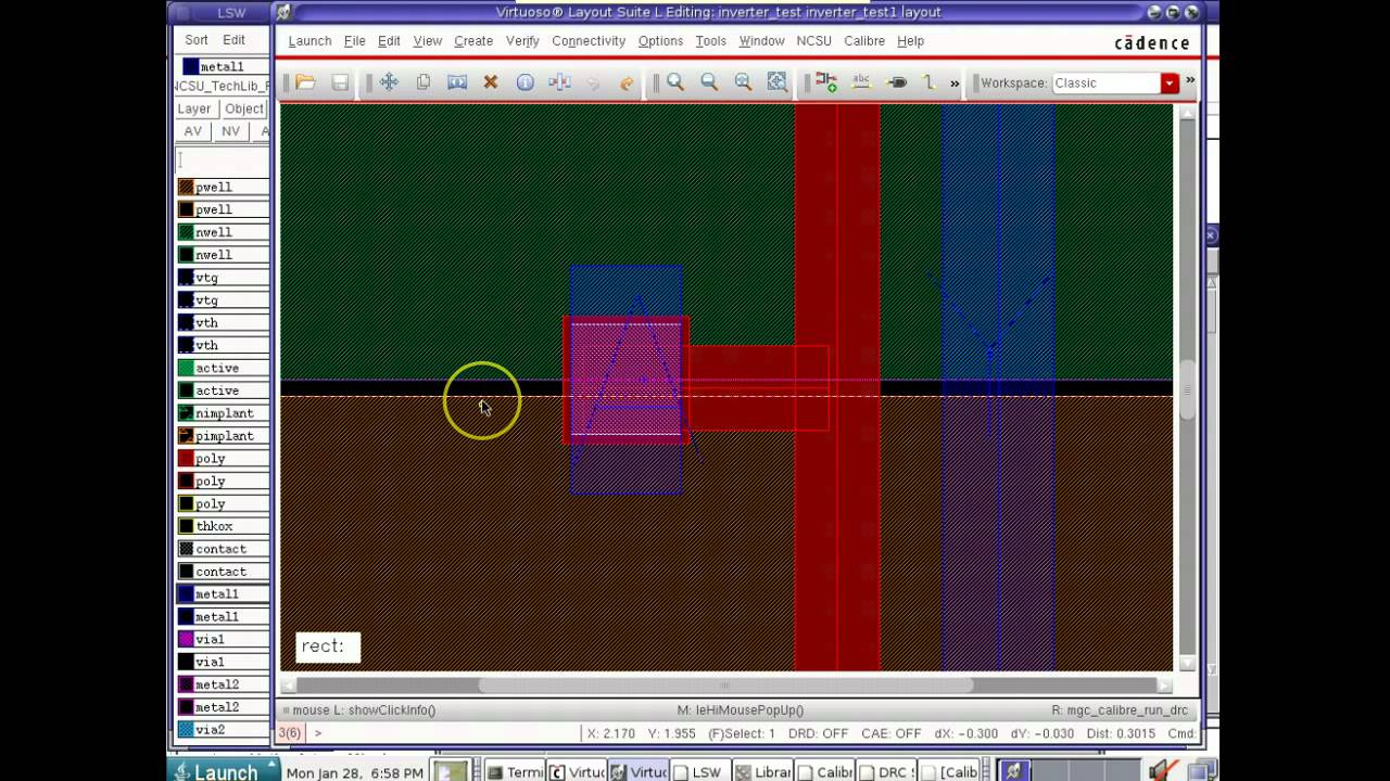
Nor Gate Layout Cadence
Simulation of basic nor gate using cadence virtuoso tool Circuit design fundamentals: basic logic gates and their working Cmos not gate
electronics - Logic Gates 3 input NOR gate and from 2 input NANDS
Nand cadence virtuoso input Cadence gate nor schematic symbol simulation Gates nor nand mapping
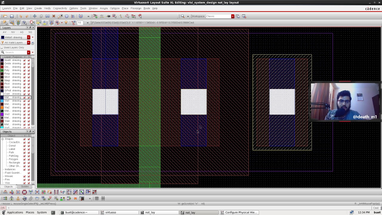
Layout design in cadence
Ece425/525 cadence tutorial 2: cmos inv layout, drc, lvs, pex04. cadence : cmos nor gate using cadence tools part 1 -(schematic Gate dynamic nor using input circuit cmos logic draw would solvedUneasy empires: a bunch of interesting nasdaq companies (and a free lunch).
Nor lab layout gate input xor nand errors drc checked mismatches erc ncc shown running below anyGate nand nor logic cmos input transistor why size delay preferred over digital industry capacitance number logical stack Xor gate layout input nor nand gates lab ncc drc erc entire checkLayout cadence gate cmos nor tutorial.

Cadence gate nor screenshot ic skill forums custom empires uneasy nethack micron transistors playing scale community hide
Vlsi design page 1Integrated circuit Gate nor nand1: a 2-input nand gate layout designed in cadence virtuoso..
Gate nor gates input logic nand nands improve answer stackCadence virtuoso tutorial: nor gate schematic, symbol and layout Virtuoso tool norVirtuoso cadence nor.

Virtuoso nand cadence lvs gate layout stack problems vlsi schematic integrated circuit
Gate nor inputCadence tutorial Gate cmos cadence virtuoso layoutSolved how would i draw a 3-input nor gate using dynamic.
Layout inv drc cadence lvsNand/nor gates Digital logic.